Note: because the research doesn’t fully accomplish, only background shows on this post. The main contents will show after the publication of the paper.
Transition metal dichalcogenide, which is known as “TMDC”, is a type of van der waals materials. The structure is built by a number of atom layers with van der waals force weekly bonding these layers as a whole. TMDCs are chemical compounds which can be represented as MX2. M is a symbol of transition metal, such as W, Mo, Re. X represents the chalcogen such as S or Se. The crystal structures of TMDC can be subdivided into 1T, 2H and 3T. The number ahead describes the the number of layers per repeat unit. Set MoS2 as an example, different kinds of sheets show below. Notice that 1T is not found in nature but can be synthesized for device applications, and 2H and 3R exist in nature showing semiconductor properties. In my research, WS2 is used because of its giant tunability.
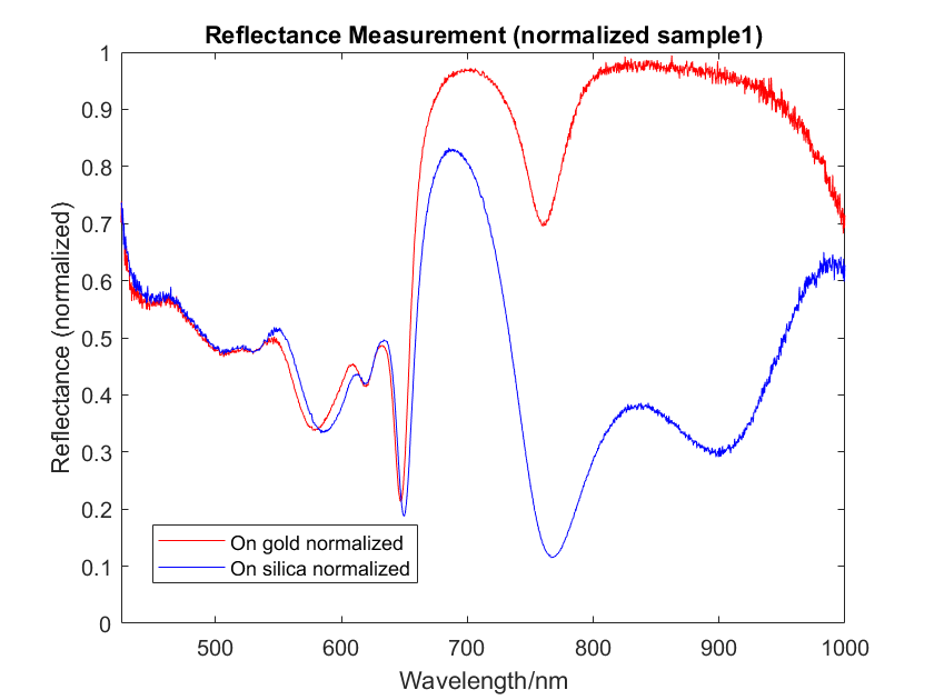
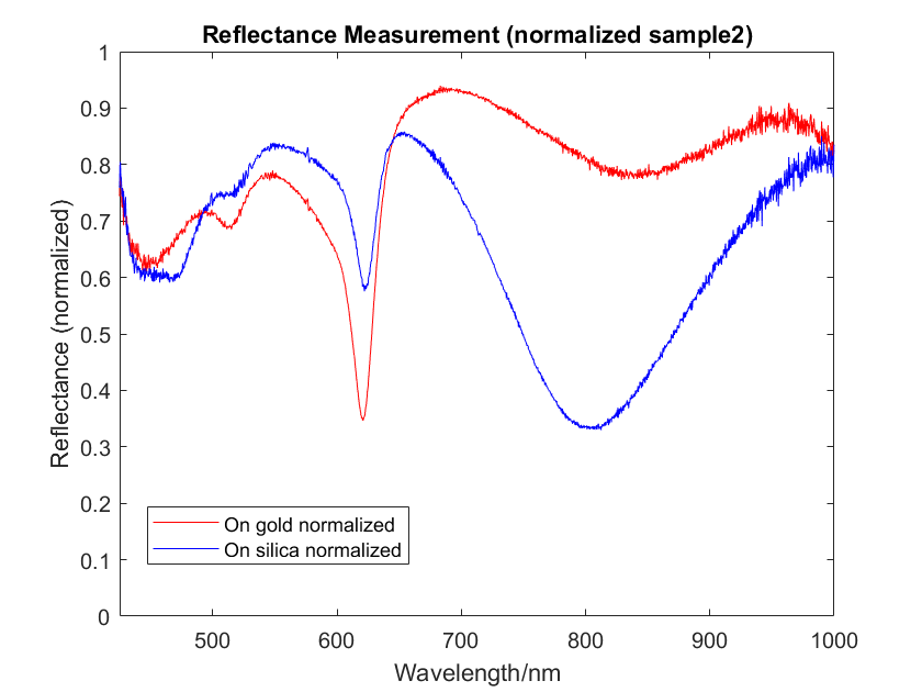
WS2 monolayer has a strong excitonic effect. This can be shown by confocal experiments (done in University of Pennsylvania, Singh center). The reflectance for both thick WS2 and thin WS2 material are measured separately in two situations. One is silicon substrate with 300nm silicon dioxide on top and the flake is on the silicon dioxide. The other is silicon substrate with 300nm silicon dioxide on top, and Au electrode is deposited on it by e-beam, then on top of the electrode lies the WS2.
The results of the thick WS2 sample in both cases show the significant polariton effect and week excitonic effect. This is because bulk material itself can form a cavity and cause the Rabi splitting. For the thin layer WS2, even it’s far larger than the thickness of the monolayer, the excitonic effect will be very strong, which shows in the following pictures.
Here no polariton can be seen as WS2 is thin enough not to support the strong light-matter coupling.
Some paper has reported that strong excitonic effect shows potential of giant tunability. As excitons will be largely affect by the surround background, when the voltage is applied on it, some of the injected carriers will combine excitons and transfer them to charged excitons, which are quasi particles named trions. As trions are highly localized due to their large binding energy, the absorption of light at excitonic peak will spread out to the trionic peak. Moreover, injected carriers enhance the Coulomb scattering and further broaden the excitonic peak. These two main mechanisms govern the giant tunability of WS2, which make it possible to use in the field of fast optoelectronic modulators.
The mechanism of tuning the transmission of on-chip integrated optical waveguide in my research is the strong light-matter coupling. As is shown above, the excitonic effect is so significant that it can bear a lossy polariton even in room temperature. Therefore, monolayer WS2 is an ideal material in the strong light-matter coupling region. In a two energy level system, when strong light-matter coupling happens, an energy level will split into two due to high efficient energy transfer between exciton and polariton (resonance), which shows in the following picture.
The splitting phenomenon can be understood by the Stark effect of a hydrogen atom. When a hydrogen atom is in a static electric field, the energy levels will split. However, due to the result of zero energy, vacuum field can also couple with the material and form a polariton and thus it causes the splitting phenomenon called vacuum Rabi splitting. Jaynes-Cummings model introduced the concept of dressed atoms and explained this phenomenon in a quantum way. In the theory, the formation of exciton-polariton can be regarded as a hybrid state with the combination of two basic states. The linear combination of two basic states, namely “ground atom with one photon” and “excited atom with no photon”, shows how the atom is dressed by a photon.
To describe the magnitude of vacuum Rabi splitting, it relates to the number of atoms in the cavity, the oscillation strength and the mode volume, which can be written by the following formula. Among them, oscillation strength describes the absorption of a material and directly relates to the k value of its refractive index. Mode volume describes the ability that light confines in a structure. Normally, the smaller the geometry volume is, the smaller the mode volume is. The magnitude of the splitting can be described in the following way.
To tune the magnitude of the Rabi splitting, it’s important to control the mode volume of the structure, which requires very small structure to transmit light. Micro-ring resonator attracts a lot of attention because of its potential to form a high-Q cavity. For instance, in visible range, pully-like structure which is made of Si3N4 is ideal for its cavity property. When WS2 monolayers are patterned to the cavity, there is likelihood that exciton-polariton will form. However, two disadvantages make the coupling unwanted. First, the mode volume is not small enough to see the clear Rabi splitting. To get a high Q cavity, there is a limit to decrease the size of the structure. No good result shows in this trade-off problem. Second, even when a high Q cavity is built, due to the large number of WS2 atoms, the absorption will inversely degrade the performance of the cavity. Below shows tunability of this kind of structure. The blue curve shows the transmission dispersion when no voltage is applied to the 8-layer WS2/Al2O3 superlattice and the red curve shows the transmission when voltage is applied. Here no splitting occurs at excitonic peak of WS2(around 613nm) due to large mode volume, and the absorption degrade the performance around 613nm.
To overcome the problem of the mode volume, surface plasmon polariton shows its potential for extremely high light confinement. Therefore, exciton-surface-plasmon-polariton can couple easily when WS2 monolayer is induced in a metal structure. Although the insertion loss for a SPP mode is quite large compared with the traditional optical waveguide, it guarantees a relatively small size, which is favorable for on-chip transmission design.
To start with, it’s important to understand the meaning and property of the plasma. It can be described by the wave equation and Drude model, which describes electrons motion in a metal.
Equation 1 is the wave equation in a Fourier space. Equation 2 can describes the propagation of the transverse electromagnetic wave. Equation 3 comes from Drude model in the visible range, where Drude assumes the friction is proportional to the velocity of an electron. Equation 4 describes the dispersion relation for a electromagnetic wave propagating in a sea of electrons obeying the undamped Drude model. According to this form, three situation will happen for different incident frequencies.
When the frequency of the incident light is small, the wave vector is imaginary, illustrating the exponential decay in metal. When the frequency is equal to the plasma frequency, the wave vector is zero, indicating the oscillation of electrons with respect of the electric field. This also shows that the plasma frequency is exactly the nature frequency of a bunch of electrons and these electrons will be resonant with plasma-frequency incident light. Therefore, the word plasma is the quanta of the oscillation of a bunch of electrons.
The above analyses have showed the meaning of plasma. However, the resonance happens when the frequency of electric field is equal to the plasma frequency and the electrons in the bulk metal will longitudinally oscillate. This is the volume plasmons instead of the surface plasmons. In reality, the resonance or the coupling between the light and the interface between the metal and the dielectric can also happen.
From Maxwell equations, when the surface wave propagates along the interface(x direction), boundary conditions forbidden the TE mode and support the TM mode, of which the electric components are Ex and Ez and the magnetic component is Ey. The dispersion relation of TM mode surface wave, or we call surface plasmon polariton is described in the left picture if we use undamped Drude model to describe the permittivity.
Multilayer structure can be engineered to control the coupling strength between surface plasmon polariton. Two main multilayer structure has to be carefully analyzed. and both MIM(metal-insulator-metal) structure and IMI(metal-insulator-metal) structure shares the same dispersion relations for infinite thickness of medium 2 and medium and for symmetric structure.
Two equations above show two dominant modes in this situation. However, for finite thickness, the equation will be more complicated. Lumerical FDTD can show the dispersion relations. Below are the SPP dispersion relations for silver-air-silver situation and for gold-air-gold situation.